Taiwan Semiconductor Manufacturing Company (TSMC) has approved an colossal $44.96 billion investment, a definitive move poised to supercharge the artificial intelligence boom. This strategic financial commitment, disclosed just recently, underscores the company’s unwavering determination to maintain its critical foundry leadership and drive the next wave of technological innovation globally. We are observing a significant inflection point in the semiconductor industry, one that will resonate through every sector reliant on advanced computing.
This substantial allocation is far more than a routine capital expenditure; it is a declaration of intent. It directly addresses the insatiable global demand for high-performance computing (HPC) and AI accelerators, chips that form the backbone of everything from generative AI models to autonomous systems. The implications for the technology landscape, from silicon design to end-user applications, are profound, setting the stage for accelerated progress.
Our editorial analysis indicates that this investment will ensure TSMC remains at the forefront of semiconductor manufacturing, providing the advanced nodes and packaging solutions necessary for the most complex AI workloads. The sheer scale of this financial backing reflects the company’s pivotal role in the global technology supply chain, acting as the indispensable engine for tech giants and innovative startups alike. The ripple effects will be felt across economies and industries.
As of February 11, 2026, the technology world stands on the cusp of an unprecedented AI era. TSMC’s strategic foresight and significant capital deployment are precisely what is needed to transition theoretical AI potential into widespread practical application. This deep dive will explore the multifaceted impact of this investment, from its technological underpinnings to its geopolitical significance, and its ultimate role in shaping our AI-powered future.
TSMC’s $44.96 Billion Bet: Fueling the AI Revolution
What is the significance of TSMC’s $44.96 billion investment? This monumental financial approval represents TSMC’s strategic commitment to reinforcing its dominant position in the semiconductor manufacturing sector, specifically targeting the burgeoning artificial intelligence market. The capital infusion is designed to expand production capacity for cutting-edge nodes and advanced packaging technologies, both of which are absolutely critical for powering the next generation of AI hardware. Without this kind of foundational investment, the rapid advancements we anticipate in AI would simply not be possible.
The AI revolution, characterized by increasingly sophisticated algorithms and data-intensive applications, demands ever-greater computational power and efficiency. Traditional chip architectures are often insufficient to meet these requirements, necessitating specialized AI accelerators built on the most advanced process technologies. TSMC, as the world’s leading pure-play foundry, is uniquely positioned to fulfill this demand, manufacturing chips for virtually every major AI innovator.
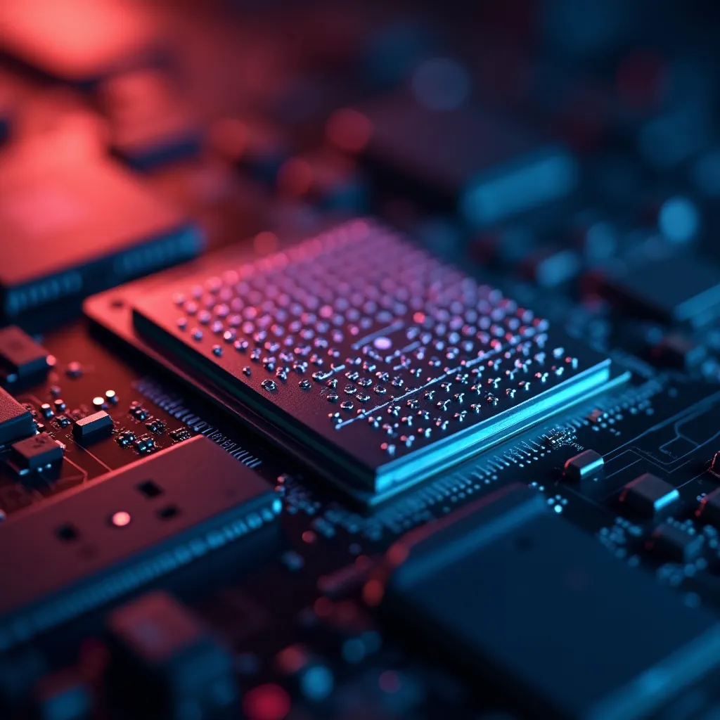
This investment is not just about producing more chips; it is fundamentally about producing *better* chips. A substantial portion of the $44.96 billion will likely be directed towards research and development for sub-2nm process technologies, such as N2 and the forthcoming A14 (1.4nm) nodes. These nodes offer significant improvements in transistor density, power efficiency, and performance, which are indispensable for designing powerful yet energy-conscious AI processors that can handle complex neural networks and massive datasets.
Furthermore, advanced packaging technologies, like TSMC’s CoWoS (Chip-on-Wafer-on-Substrate) and InFO (Integrated Fan-Out) solutions, are becoming as crucial as the logic process itself. These innovations allow for the integration of multiple chiplets and High Bandwidth Memory (HBM) into a single, high-performance package, dramatically increasing interconnect speeds and reducing power consumption. Such packaging is essential for AI accelerators that require tightly integrated compute and memory resources to avoid data bottlenecks. We observe a clear strategic intent here.
The demand landscape for AI chips is incredibly diverse, spanning hyperscale data centers, edge devices, autonomous vehicles, and even novel applications in areas like AI Forecasting Models: Crypto Markets’ Ultimate Testbed 2026. Each of these segments has unique requirements, but all converge on the need for smaller, faster, and more power-efficient silicon. TSMC’s investment is meticulously planned to address this broad spectrum of needs, ensuring a robust supply chain for the entire AI ecosystem. This foresight is what separates market leaders from followers in this intensely competitive arena.
The scale of this capital expenditure also reflects the sheer cost and complexity of modern semiconductor manufacturing. Building a single state-of-the-art fabrication plant (fab) can cost tens of billions of dollars, requiring highly specialized equipment, advanced materials, and an immense pool of engineering talent. TSMC’s $44.96 billion is thus a necessary investment to keep pace with technological advancement and continue meeting the escalating demands of its clientele in the AI space. This positions the company firmly as the bedrock of global technological progress.
The Anatomy of a Semiconductor Giant’s Strategy
What specific areas will TSMC’s $44.96 billion investment target? Our analysis suggests that this colossal sum will be strategically deployed across several critical vectors: advanced process technology R&D and manufacturing capacity expansion, particularly for sub-2nm nodes; cutting-edge packaging solutions; and global manufacturing footprint optimization, including regional diversification. These pillars collectively support TSMC’s ambition to remain the indispensable foundry for AI chips.
A significant portion of the capital will undoubtedly be allocated to the development and ramp-up of TSMC’s next-generation fabrication processes. The move towards N2 (2-nanometer class) technology and beyond is paramount for AI chips, which require billions of transistors packed into incredibly small areas to deliver unparalleled performance. This involves not only perfecting the extreme ultraviolet (EUV) lithography techniques but also exploring novel transistor architectures, such as Gate-All-Around (GAA) transistors, which are essential for further scaling. These advanced processes are complex and incredibly capital-intensive to develop and implement in high-volume manufacturing.
“TSMC’s commitment to such a substantial investment is not merely about capacity expansion; it’s a strategic assertion of intellectual and technological dominance,” states Dr. Lin-Sung Chou, Head of Advanced Materials Research at National Tsing Hua University. “We are witnessing the foundational build-out for the next decade of AI, where power efficiency and extreme density will be paramount. Their focus on both advanced nodes and packaging solutions demonstrates a holistic understanding of future compute challenges.” This expert perspective highlights the dual focus required for AI innovation.
Beyond the core logic processes, advanced packaging solutions are receiving unprecedented attention. As chiplets become more prevalent and the need for higher bandwidth between logic, memory, and specialized accelerators intensifies, innovative packaging like 3D stacking and chip-on-wafer technologies are becoming performance differentiators. TSMC’s investments here will likely expand its CoWoS and InFO capacities, ensuring that multi-chip modules can be integrated efficiently and reliably. This capability is absolutely crucial for the complex architectures seen in modern AI GPUs and custom ASICs.
The geopolitical landscape also plays a significant role in TSMC’s investment strategy. While Taiwan remains its primary manufacturing hub, efforts towards global diversification, including fabs in Arizona and Japan, are part of a broader strategy to mitigate supply chain risks and cater to regional demands. While the $44.96 billion is primarily focused on core technological advancement, aspects of this will inevitably support the infrastructure and R&D for these overseas operations, ensuring a resilient global semiconductor ecosystem. This strategic diversification helps to hedge against potential disruptions, reflecting lessons learned from recent global events.
Our analysis also shows a keen focus on sustainability and automation within new fab builds. With energy consumption being a growing concern for data centers, TSMC is investing in more energy-efficient manufacturing processes and facilities. Furthermore, increased automation and AI-driven predictive maintenance within its fabs will enhance operational efficiency, reduce human error, and accelerate production cycles, further solidifying its manufacturing prowess. This comprehensive approach underscores a commitment not just to volume, but to intelligent and sustainable growth.
This substantial capital outlay positions TSMC not just as a contract manufacturer, but as a critical enabler of the entire global technology roadmap. It ensures that the most ambitious designs from companies like NVIDIA, AMD, Apple, and Google, particularly those targeting AI, have a clear and reliable path from design to mass production. This reinforces TSMC’s indispensable role in the current technological paradigm, making it the quiet powerhouse behind many of the innovations we now take for granted.
Operationalizing AI Dominance: From Wafer to World-Changing Chips
How will TSMC’s investment translate into tangible outcomes for the AI industry? This massive financial commitment will directly result in an accelerated pace of innovation, increased availability of high-performance AI chips, and the proliferation of AI capabilities across numerous industries. From the moment a silicon wafer enters a TSMC fab to the point a finished chip powers a complex AI model, the impact of this investment will be evident at every stage.
The most immediate and critical outcome will be the surge in manufacturing capacity for advanced AI processors. As the demand for AI computation continues its exponential rise, particularly for large language models (LLMs), generative AI, and advanced analytics, existing capacities are constantly strained. This investment will alleviate those bottlenecks, enabling AI companies to scale their deployments faster and bring new AI-powered products to market with greater agility. This means more accessible and powerful AI tools for businesses and consumers alike.
Improved process technologies will also mean that AI chips become even more powerful and energy-efficient. A 2nm or 1.4nm chip can perform significantly more calculations per watt than its 3nm or 5nm predecessors. This translates into lower operational costs for data centers running vast AI workloads, and longer battery life for edge AI devices, such as those found in smart homes, industrial IoT, and autonomous vehicles. The implications for sustainable AI are quite significant, reducing the environmental footprint of ever-growing compute demands.
“Our analysis shows that this $44.96 billion allocation is a calculated move to maintain a significant lead in the foundry space, particularly against emerging regional players and existing competitors,” explains Ms. Anya Sharma, Lead Analyst at Semiconductor Insights Group. “It sends a clear message to their key customers – the AI titans – that TSMC is prepared to scale their most ambitious designs, ensuring a bottleneck-free pathway to market for their innovative AI hardware. This investment secures critical future revenue streams.” Her insights confirm the strategic importance of this financial maneuver.
This increased capability and efficiency will unlock new possibilities for AI applications. Imagine self-driving cars with even faster, more reliable real-time decision-making, powered by specialized TSMC-made chips. Consider medical diagnostic tools that can process complex imaging data instantly on a portable device, rather than requiring cloud connectivity. The ability to integrate powerful AI locally, at the “edge,” will revolutionize many sectors. Even seemingly unrelated fields, such as the discoveries made by Underwater Robot Unearths Unbelievable Decades-Lost Discovery on Seabed, rely on advanced computing to process and interpret vast amounts of sensor data efficiently.
Moreover, the investment will support the development of custom AI silicon. As AI workloads become more specialized, generic processors often fall short. Companies are increasingly designing their own custom AI accelerators, and they rely on TSMC to bring these designs to life. This funding ensures TSMC has the capacity and expertise to handle a diverse array of custom chip projects, fostering a broader ecosystem of AI innovation rather than a centralized one. It allows for highly optimized solutions tailored to specific AI challenges.
The capital injection will also indirectly benefit the broader technology ecosystem by fostering innovation in related industries, from electronic design automation (EDA) software to advanced materials and equipment suppliers. As TSMC pushes the boundaries of manufacturing, its partners are compelled to innovate alongside it, creating a virtuous cycle of technological advancement. This interconnected growth ensures that the entire chain strengthens, benefiting everyone involved and accelerating the pace of change.
The AI-Powered Horizon: TSMC’s Vision for 2030 and Beyond
What does TSMC’s $44.96 billion investment signify for the long-term future of AI and semiconductor technology through 2030 and beyond? This substantial capital infusion lays the groundwork for pervasive AI integration across society, ensuring that the physical infrastructure for increasingly powerful AI systems remains robust and capable. We foresee a future where TSMC’s advancements enable ubiquitous AI, from smart dust to exascale supercomputers, fundamentally reshaping our interactions with technology and the world.
By 2030, we expect to see the widespread adoption of AI in every conceivable industry, largely due to the foundational work done by companies like TSMC. The investment in sub-2nm nodes, for instance, will enable a new class of AI chips that are not only faster but also consume dramatically less power. This efficiency is critical for the expansion of AI into edge devices, allowing sophisticated AI to run locally on smartphones, wearables, and embedded systems without constant cloud connectivity. This shift towards localized AI enhances privacy, reduces latency, and opens up entirely new application domains.
The move towards advanced packaging, including 3D stacking and chiplet architectures, will become the norm for high-performance AI compute. This will allow for highly specialized, modular AI processors that can be customized for specific tasks, from natural language processing to computer vision, delivering unprecedented levels of parallelism and data throughput. Such architectural innovations will become key differentiators, even more so than raw transistor count, pushing the boundaries of what is possible with silicon. This future architecture promises immense flexibility.
Geopolitical considerations will also continue to shape TSMC’s strategy. The current focus on securing and diversifying supply chains remains paramount. As nations increasingly view semiconductor manufacturing as a matter of national security, TSMC’s distributed R&D and manufacturing capabilities, partially supported by this investment, will become vital. While economic factors drive much of the investment, ensuring technological independence and access becomes a critical strategic imperative, especially in light of developments such as China Extends Crypto Ban: Stablecoins & Tokenized Assets Blocked, which underscore the complexities of global tech policy.
Looking further, TSMC’s continued investment in fundamental research means exploring materials beyond silicon, such as graphene or carbon nanotubes, and novel computing paradigms like quantum computing. While these are long-term horizons, the capital approved today indirectly funds the underlying research capabilities and talent acquisition necessary to even contemplate such shifts. The company is not merely optimizing current technologies; it is actively investing in the pathways to future breakthroughs, ensuring a continuous pipeline of innovation for decades.
The impact on software development cannot be overstated. As hardware becomes more capable and efficient, software developers gain unprecedented freedom to create more complex, intelligent, and resource-intensive AI models. This synergistic relationship between hardware and software will accelerate the development of truly transformative AI, leading to advancements that are difficult to fully predict from our current vantage point. The potential for innovation, including new White-Label Crypto Exchange Trends for Token Startups in 2026, depends heavily on accessible and powerful computing infrastructure.
The Bottom Line: Securing the Future of Global Innovation
TSMC’s approval of $44.96 billion to lead the artificial intelligence boom is a pivotal moment for global technology, securing the foundational infrastructure for future innovation. This monumental investment underscores the company’s indispensable role as the primary engine for advanced semiconductor manufacturing, a role that will only grow in significance as AI permeates every facet of our lives. We have analyzed how this capital injection is strategically targeted at the bleeding edge of process technology, advanced packaging, and operational efficiency, all critical for the next wave of AI development.
The scale of this commitment reflects not just TSMC’s financial might but also its deep understanding of the semiconductor industry’s future trajectory. It is an investment in billions of transistors, in the precision of atomic-level engineering, and ultimately, in the intellectual capacity that drives human progress. Without such bold and sustained capital deployment, the exponential growth of AI would inevitably face severe bottlenecks, hindering the pace of discovery and application across countless domains. The world’s reliance on TSMC’s capabilities continues to grow with each technological leap.
From powering sophisticated generative AI models to enabling highly efficient edge AI devices for everyday use, TSMC’s chips are the silent workhorses of the digital age. This $44.96 billion ensures that these workhorses remain at the forefront of performance and efficiency, fueling everything from scientific breakthroughs to economic growth. It is a testament to the fact that while software defines AI’s intelligence, hardware determines its reach and its power to transform. The impact will be global and long-lasting, solidifying TSMC’s legacy for decades to come.
The ripple effects of this investment will extend far beyond Taiwan’s borders, impacting global supply chains, fostering international technological cooperation, and setting new benchmarks for manufacturing excellence. As the AI landscape continues to evolve at breakneck speed, TSMC’s foresight and financial commitment stand as a beacon, guiding the industry towards a future where intelligence is not just artificial, but universally accessible and transformative. This decision cements its role as the backbone of our AI-driven world, ensuring continued progress.